Recently, a research team led by Professor Huo Nengjie from the School of Electronic Science and Engineering (School of Microelectronics) at South China Normal University Faculty of Engineering has achieved a breakthrough in the field of short-channel vertical transistors for CMOS inverters and digital logic circuits. Their findings, entitled "Self-aligned vertical short-channel 2D transistors for CMOS inverter and digital logic circuit," have been published in the prestigious international journal Materials Science and Engineering: R: Reports (a CAS Q1 Top journal with an impact factor of 31.6). Yiheng Wang, a second-year master's student at the School of Electronic Science and Engineering (School of Microelectronics), is the first author of the paper, with Professor Huo Nengjie serving as the corresponding author. South China Normal University is listed as the primary affiliation. Through innovative device architecture design, the study introduced a low-cost self-aligned etching technique, successfully fabricating high-performance vertical short-channel transistors (VFETs) and their arrays (2×8). The research demonstrated their application in CMOS inverters and logic circuits, overcoming the limitations of traditional lithography processes and providing a new paradigm for integrated circuit development in the post-Moore era.
Technical Innovation: Self-Aligned Etching Technique Breaks Through Nanofabrication Bottlenecks
Currently, most research relies on electron-beam lithography (EBL) for precise nanoscale patterning. However, this technique involves expensive equipment and high costs, limiting its use to small-scale or single-device fabrication and posing significant challenges for process scalability. For the advancement of practical applications, a well-controlled and CMOS-compatible manufacturing process for large-scale, high-density 2D vertical short-channel transistors has remained elusive.
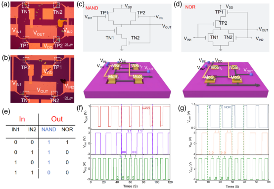
To address this, the research team developed a method involving sequential etching of metal and silicon dioxide substrates, followed by metal redeposition. This process successfully creates a vertical metal-SiO₂-metal mesa structure. Using this controllable SiO₂ mesa etching technique, the team fabricated vertical short-channel transistors with a channel length (Lch) of approximately 150 nm, demonstrating the potential to scale Lch below 30 nm. The developed self-aligned MoS₂ vertical short-channel transistors exhibit remarkable performance, including a high on-state current (>70 µA/µm) and a large on/off ratio (>10⁸), alongside significantly reduced subthreshold swing (SS) and hysteresis window. Furthermore, based on these self-aligned vertical transistors, the team successfully demonstrated fundamental logic gates such as inverters, NAND gates, and NOR gates. These results highlight the technology's strong potential for application in miniaturized advanced electronic circuits.

Application Prospects: Integrated Arrays and Logic Applications
The self-aligned vertical short-channel 2D transistors presented in this work combine a high on/off ratio, low subthreshold swing, and excellent device uniformity, demonstrating strong compatibility with large-scale integrated circuits. Based on N/P-type VFETs fabricated from MoS₂ and WSe₂, the devices not only achieve high drive current and superior short-channel control but have also been successfully used to construct high-gain CMOS inverters and low-power digital logic gates (NAND and NOR), confirming their feasibility and stability in fundamental digital logic circuits. Furthermore, 2×4 and 2×8 device arrays were designed and fabricated on the same material substrate, demonstrating the favorable process compatibility and scalable integration potential of the proposed device architecture. Given the inherent potential of 2D materials for large-area growth and heterogeneous integration, this work provides crucial technological support and a viable development pathway for realizing next-generation, low-cost, low-power, high-density logic chips and other advanced integrated systems.


This research work has been consistently supported by the National Natural Science Foundation of China, the Natural Science Foundation of Guangdong Province, and the Guangdong Provincial Key Laboratory of Chip and Integration Technology. A patent application has been filed for the related technology.
Link: https://url.scnu.edu.cn/record/view/index.html?key=93aedc911f37d3bd774952396b066cfd
